TECHNOLOGY
Application Issues
What is gettering and how does MDZ® help?
The management of metal contamination is one of the most important aspects of successful integrated circuit manufacture. Gettering has long been an important part of this. Put simply, gettering is a stand-by process whereby metal contamination is rendered harmless in the event of a failure of process contamination control. The bones of these processes are built into silicon wafers with variable degrees of success.
Gettering fundamentals
The most important metal contaminants in silicon are iron, nickel and copper, with copper being perhaps the most dangerous of all. We will illustrate both the main problems with metals and the mechanisms that lie behind the main gettering effect using copper as our example. The behavior of a metal like copper in silicon can easily be imagined by drawing a comparison to our common experience with gases dissolved in liquids. Carbon dioxide in beer, for instance. Copper diffusion in solid silicon in fact has much in common with diffusion in liquids; it is extremely fast and it’s diffusivity is not strongly temperature dependent (at least until at or below room temperature). Copper has a rather high solubility at typical process temperatures. Silicon can soak up quite a bit of the stuff when hot. This means that any copper in contact with the wafer surface (originating, for instance, from an improperly cleaned surface or diffusion boat) is rapidly dissolved and uniformly distributed into the wafer at high temperature – within seconds at 1000 degrees C for example. (It’s important to remember that at low temperatures -- in spite of its high mobility -- copper will not appreciably dissolve into silicon. It is constrained by a low solubility –- there are however exceptions: CMP under certain conditions for example). But back to high temperature copper solutions. Upon cooling -- and this is the important point -- the solubility of copper in silicon drops rapidly. Depending upon the amount of copper actually dissolved in the silicon wafer, at some point (that is to say at some temperature) during the cooling of the wafer a copper solution will become supersaturated and progressively more so upon further cooling. At some point we get so far from equilibrium that copper precipitates out of solution and the system relaxes toward equilibrium. The form that these precipitates take is that of a copper silicide: Cu3Si. These are very damaging things.
To get a feel for what is happening in a silicon wafer at this point, consider our beer analogy. A closed pressurized bottle contains a certain concentration of carbon dioxide (the silicon wafer with a copper solution at high temperature). Opening the bottle releases the pressure, and the carbon dioxide solution -- which was perfectly happy at high pressure -- becomes rapidly supersaturated under the new, lower pressure, conditions (the copper contaminated silicon wafer during cooling). In our bottle, in what seems no time at all after flipping the lid, bubbles form (copper precipitates). But anyone who has ever looked at a beer bottle, or the glass into which the beer was poured, knows perfectly well that the bubbles don’t form just anywhere. They form at the surface of the glass. The ones present in the liquid have merely been released from the glass surface and float to the top – this is where solids and liquids part company. The reason for the location of the bubble formation is because the formation of bubbles at the glass surface is easier (requires less energy or driving force) that in the uniform liquid. Broadly speaking this is called heterogeneous precipitation. Rain happens this way. And the same thing happens to copper in silicon.
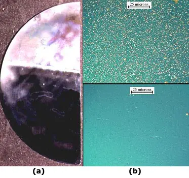
An illustration of the phenomenon of surface precipitation of copper in the absence of effective gettering. Here a half-wafer has been contaminated with copper and then heated to 900 degrees C and cooled. After the heat treatment, the bottom half (below the bright line) was then angle etched with a non-defect delineating etch to an average depth of only about 2.5 microns below the surface. Then the entire sample was then defect etched to reveal copper silicide precipitates. These are found only in the upper half of the sample (seen here in (a) as a "haze" resulting from light scattering off a very high density of etch pits). In the lower half, the surface precipitates where etched away prior to the defect delineation. (b) shows illustrative micrographs of the etch pit structure in the two halves.
Assume for the moment that we have a perfect, crystalline silicon wafer who’s only defects happen to be that the perfect crystal is truncated by two flat, parallel surfaces and that it contains a certain concentration of copper at high temperature. Upon cooling this system we will reach a temperature (typically about 300-500 degrees C, depending on the copper concentration – the wafers are out of the furnace at this point!) when the dissolved copper can no longer be held in solution. Just like in our beer glass, precipitates form very, very rapidly, even explosively, on the wafer surfaces equally -- and nowhere else. This happens to be a very unfortunate fact for integrated circuit technology. One of these vulnerable surfaces is of course where the entire investment in the processed wafer lies. The precipitation of copper in silicon is a catastrophic event. Cu3Si precipitates create enormous stresses in the silicon, generating dislocations which can extend far beyond the precipitate itself, generally creating havoc in a localized area. All manner of device failure can occur.
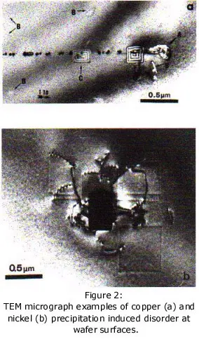
TEM micrographs illustrating the kind of mess a surface copper and nickel precipitation events can make.
But there’s an upside to all of this, or rather, an advantage can be taken of what’s going on here. As we have seen in the example above, a free silicon surface is a more preferable site for metal precipitation than a perfect bulk. (A free surface contains atomic steps and there is an entire half space in which the precipitate growth is unconstrained by the crystal lattice). This differential in barriers to precipitation has important consequences for the final spatial distribution of the precipitates in a wafer -- just as in the beer glass. By preferential in the silicon wafer case, what we really mean is that a precipitation event can happen at a higher temperature, in other words before some other precipitation event could happen; less under-cooling is required to drive the reaction. Now, in such a rapidly diffusing system as copper (or nickel) in silicon, this means that, in practically no time at all (on the order of seconds, really), once the nucleation of the metal precipitates begins (at the wafer surface in this example) the growing surface-nucleated precipitates consume essentially all of the dissolved metal in the wafer. This means that there is no chance for metal to precipitate anywhere else. In effect, precipitation has been suppressed everywhere but at the preferential sites.
Harnessing this preferential precipitation and the associated location-specific suppression of precipitation in an appropriate way is the essence of most practical gettering systems.
So now if, for whatever reason, process controls have failed and metal has been introduced into a silicon wafer our goal is to insure that the precipitation of that metal at the sensitive front surfaces is robustly and reliably prevented. This is the main job of gettering. Much has been written about gettering in the last 25 years or so, but in essence it all boils down to this. Now we’ve already seen that a normal surface is itself a preferential site for precipitation. It follows from the above argument that all we have to do to suppress precipitation there is to create a condition in the wafer -- somewhere other than at the wafer front surface -- which is more preferable. That is, we must create sites at appropriate locations in the wafer where the barrier to metal precipitation is still lower than that of the already low barrier free surface. This is easy.
So that’s all there is to it. Well, almost. Now, just because metal has precipitated somewhere following a heat treatment doesn’t mean that it will stay there. Metal silicide precipitates are not stable at high temperatures. Although we won’t return to this point in this brief discussion, it’s worth keeping in mind here that each time the wafer is reheated they dissolve and the whole procedure begins anew [1,2]. Gettering is a dynamic process.
Practical gettering systems: external systems
A simple way to lower the barrier to metal precipitation at a free surface is to create disorder of nearly any kind in it. If this is applied to the back surface of the wafer only then a differential between the front and back surface is achieved which alters the balance in the metal precipitation preferences between the two surfaces. Over the past 30 years or so many different back surface disordering processes have been applied to silicon wafers to achieve preferential metal precipitation at the back surface and thus effective suppression of precipitation at the front surface. Since the metal is precipitated at the back surface rather than in the bulk of the wafer (see below) such systems are called external gettering (EG) systems. Almost any kind of damage to the wafer back surface will achieve this result. The first external gettering system used in large volumes was a backside damage achieved by abrading the surface with sandpaper – an almost unbelievably crude method from today’s perspective. Refinements to this over the years included laser damage, sand blasting and a more politically correct (from an IC processing point of view) CVD deposition of a highly disordered poly-silicon film applied to the backside. Backside ion-implantation damage has also been used. Several of these techniques are still in use today and to great advantage. But there are several disadvantages to these external gettering approaches which will no doubt limit or eliminate their applicability in advanced IC applications. The first requirement is that damage applied to wafer back-surfaces should live throughout the entire IC process. This is not necessarily a given. In addition to this, the disordering processes should themselves be device defect neutral. This is also not necessarily to be taken for granted. The sand-blasting of silicon surfaces is known to create particle-generating sources which can result in the transfer of particles from the back side of silicon wafers to the front side of adjacent wafers in a diffusion boat, thus in some cases causing more damage than it sought to prevent. Poly-silicon backside coatings can be oxidized away and are certainly not applicable in future double-side polished wafers.
Practical gettering systems: internal systems
Essentially all silicon wafers for IC applications are grown by the Czochralski (CZ) method. An important difference between this method and the Floating Zone (FZ) method is that the silicon melt is contained in a quartz crucible. The main result of this is that oxygen from the crucible is unavoidably dissolved into the molten silicon and incorporated in the solid crystal ingot in rather high concentrations. For a variety of reasons, the rather low mobility of oxygen in silicon being one, this excess oxygen can precipitate homogeneously, that is, at arbitrary sites, in a silicon crystal. This can occur during the cooling of the crystal during growth and in subsequent wafer heat treatments during use. Oxygen precipitates in bulk, or interior, of silicon wafers create disorder which can effectively lower the barrier for the subsequent precipitation of metals just like disorder on the wafer surface. The potential for using bulk oxygen precipitates as a gettering mechanism was first proposed in 1977 [3] although the mechanisms were not clear at the time. In fact, it is known [4] that even very tiny oxygen precipitates at very early stages of growth (too small to observe by the conventional etching techniques normally used to see them) can result in energy barriers lower than that of a free surface and thus offer the potential for very effective suppression of surface precipitation and thus gettering. On the surface of things, the use of oxygen precipitates to control metal precipitation is a very attractive idea. A huge effort has been extended in the years since the realization of this effect to harness the potential of bulk oxygen precipitates to manage metal contamination. Such an approach to gettering is called internal gettering (IG).
The IG approach clearly side-steps the issues of particle contamination and damage longevity. But the use of oxygen precipitates as a gettering system can be a dangerous plaything. The engineering challenge is to insure that sufficient densities of oxygen precipitates are robustly and reliably produced in arbitrary IC processes and that a surface layer free of oxygen precipitates (a denuded zone) is produced in the wafer during the processing of the wafer. The denuded zone is required to avoid the presence of oxide precipitates in the near surface device layer in order to avoid detrimental effects of oxygen precipitates themselves. This is usually achieved by causing the dissolved oxygen in the wafer to out-diffuse at high temperature prior or during the nucleation of the oxygen precipitates in the bulk. This is often a costly additional process step which serves no other purpose than to prepare the wafer for use. A sufficient density in the bulk of the silicon wafer is required. This is to insure that, once metal precipitation starts at the oxide precipitate sites, these volume distributed sinks for metal diffusion are of a sufficiently high density to insure that a sufficient suppression of the metal concentration near the front surface in order to suppress metal precipitation there. It is known that oxygen precipitate densities of about 1-5 x 10 8 cm-3 are required for this [5,6]. An example of an ideal depth distribution of oxygen precipitates for gettering purposes is shown in Figure 3. Illustrated is a defect etched cross-section of a processed silicon wafer. The surface of the wafer is at the top. The depth of the defect free denuded zone is about 80 microns and the bulk density of oxygen precipitates is about 8 x 10 9 cm-3.
The engineering challenge of internal gettering
The engineering challenge to reliably produce such internal gettering structures has often proven to be illusive or expensive, or both. The general problem of the physics of the precipitation of oxygen in silicon has proven to be hugely complex and remains a still wildly unsatisfactorily resolved problem. In the 20 or so years since the discovery of the IG effect in silicon wafers, many scientists and engineers have struggled with the problem of precisely and reliably controlling the precipitation of oxygen in silicon which occurs during the processing of wafers into integrated circuits. This has been met with only partial success in the sense that the "defect engineering" of conventional silicon wafers is still, by and large, an empirical exercise. It consists largely of careful, empirical tailoring of wafer type (oxygen concentration, crystal growth method, and details of any additional pre-heat treatments, for example) to match the specific process details of the application to which they are submitted in order to achieve a good and reliable IG performance. In conventional silicon wafers the resultant oxygen precipitate density profiles are wildly dependent on the details the crystal growth process (primarily crystal cooling rates), the oxygen content of crystals and the details of the IC process to which the wafers are submitted. As a result, an entire industry-within-an-industry has sprung up built around attempts to control and tailor the oxygen precipitation performance of silicon wafers to specific processes. A large proportion of the complexity (and hence cost) of the manufacture of silicon wafers is centered on the specification and control of oxygen concentration and its behavior. Once a process is known to work for a given application a kind of process rigidity sets in. The potential for cost saving process improvements are reduced. Armies of expensive applications engineers and their counterparts at IC houses work on the tailoring of oxygen concentration and crystal growth processes to meet the needs of specific silicon applications. These are costs which the industry can no longer bear.
References
- R. Falster, Z. Laczik, G.R. Booker, A.R. Bhatti and P. Török, in: Materials Research Society Symposium Proceedings Volume 262, Silicon Defect Engineering in Semiconductor Growth, Processing and Device Technology, (S. Ashok, J. Chevallier, K Sumino and E. Weber, eds., Pittsburgh, 1992), p. 945.
- [2] R Falster, in the proceedings of the satellite symposium to ESSDERC 93 Grenoble, Electrochemical Society Proceedings Volume 93-15, Ed. by BO Kolbesen, P Stallhofer, Cor Claeys and F Tardif (1993), p.149.
Although the silicon wafer is strong at room temperature, it becomes weaker as the temperature is increased. During the furnace processing steps that are necessary for the fabrication of integrated circuits (ICs), a nonuniform elevated temperature produces a nonuniform expansion within the wafer and the resulting thermal stress can cause local or widespread furnace slip. This disrupts the silicon crystal structure and permanently degrades the electrical and physical characteristics of the wafer. The dislocations that are produced by slip can cause junction leakage, premature breakdown, gate oxide integrity failure, and other problems. The physical deformation of the wafer can cause pattern misalignment, focus, and chucking problems, as well as wafer breakage.
A nonuniform temperature is produced in the wafer during furnace push and temperature ramp-up as the radiant energy from the furnace tube heats up the wafer edge faster than the wafer center. This can cause slip around the wafer edge and warp the wafer into a saddle shape (Figure 1).
During temperature ramp-down and furnace pull, the wafer cools faster at the edge than in the center, and this temperature nonuniformity can create slip in the wafer center and cause the wafer to bow (Figure 2).
Decades of fabricating ICs on silicon wafers have shown that furnace slip is always a problem. This is because the fabrication engineer is always faced with the conflicting goals of increasing the speed of furnace temperature ramps and push-pull steps to maximize the furnace throughput, while at the same time limiting the speed of temperature ramps and push-pull steps to prevent wafer warpage and the creation of yield-killing slip dislocations. Each time the wafer diameter increases, a new balance must be found. Each time a new IC technology creates additional built-in device stress, the balance shifts.
For example, when oxide-filled shallow trench isolation (STI) structures were introduced, furnace recipes which had previously produced slip-free wafers became recipes which produced massive furnace slip. During thermal cycling, the stress the oxide exerted on the trench side-walls plus the thermal stress due to temperature nonuniformities in the wafer added together to create slip dislocations and to move those dislocations into leakage-sensitive parts of the IC device. But by moderating both the built-in IC device stress and the furnace stress, IC devices with STI structures are now being fabricated successfully.
Temperature is primary factor that controls the strength of the silicon wafer, and this must be taken into account when setting furnace push/pull and temperature ramping conditions. The strength of the wafer decreases significantly at its temperature is increased from 750°C to 800°C. If wafers are pushed into or pulled from a furnace tube set at 750°C, wafer slip is almost never a problem, but if they are pushed or pulled with the tube set at 800°C, slip is almost always a problem. The strength of the wafer decreases further as its temperature is increased further. To prevent wafer slip during furnace temperature ramping, it is necessary to use lower and lower ramping rates for higher and higher temperature ranges. Recommended ramp rates for 200 mm wafers are given in "How to Prevent Furnace Slip." Smaller diameter wafers can be ramped slightly faster, but 300 mm wafers must be ramped more slowly.
Other factors also affect the strength of the silicon wafer. The higher the density of dislocations in a wafer, the weaker the wafer. It takes a considerable stress to create a dislocation, but it only takes a small stress to cause an existing dislocation to move or multiply. The higher the interstitial (dissolved) oxygen concentration, the stronger the wafer. Interstitial oxygen atoms attach themselves to dislocations and prevent them from moving or multiplying. However, the higher the amount of precipitated oxygen, the weaker the wafer. Growing oxygen precipitates use up the interstitial oxygen and punch out new dislocations. The higher the concentration of dopant atoms, the stronger the silicon wafer. The strain fields around atoms, which are larger or smaller than the silicon atoms, impede the motion of dislocations. IC films can exert stress on the underlying silicon and make slip more likely. Trench and other IC structures, as well as mechanical damage sites, weaken the wafer by acting as stress concentrators.
Even though the silicon wafer is weakened by IC fabrication processing, high yielding IC processing is certainly possible if one pays attention to furnace slip and wafer strength issues.
A broken wafer is a loss and an opportunity. When a wafer breaks during fab processing, the first impulse is to clean up the mess and trash the broken pieces. But the fracture markings on the broken edges actually represent a detailed recording of the rapid sequence of events that took place during the breakage event. By examining the fracture markings with a microscope, it is often possible to discover how and why the wafer broke so that appropriate corrective and preventive actions can be taken.
The Fracture Analysis Procedure below outlines the analysis procedure and gives two references where instructive descriptions and sample photos and drawings can be found. The photos on this web page show samples of the most commonly encountered fracture markings, rib lines and tear marks. The photo captions tell how to interpret rib lines and tear marks and describe four cases where fracture analysis was useful in solving a wafer fab breakage problem.
A wafer begins to break apart when the silicon at some surface location is subjected to a sufficiently large tensile stress. The tensile stress can arise due to wafer bending, uneven cooling, penetration, or during an impact when the silicon is compressed in one direction but pulled apart in other directions. The stress required to break a wafer is greatly reduced if the wafer surface has a stress concentrator such as a preexisting crack.
The goal of fracture analysis is to discover how and why a wafer broke so that future occurrences can be prevented. If a wafer broke because of a weakness, such as a scratch that occurred at a prior processing step, then that weakness can be eliminated. If a wafer broke because it was bent or penetrated by a piece of wafer handling equipment, then that equipment can be adjusted. A broken wafer is not only a loss but an opportunity for improvement.
Fracture Analysis Procedure
- Collect samples without destroying the evidence.
- Use a scale drawing to record and report the results.
- Examine the fracture markings on the broken edges to determine the direction of travel for each crack that split the wafer apart.
- Trace the crack(s) back to the approximate origin of the breakage.
- Examine the fracture markings to determine the exact origin.
- Examine the silicon at and around the origin for evidence of why the wafer broke.

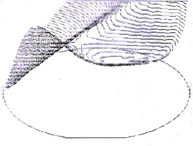
Edge chip. The curved ripples on the fracture surface are rib lines. Rib lines are produced when the leading edge of the craft that is splitting the silicon apart wanders upward and downward as it travels along. Rib lines show where the leading edge of the crack was at successive instants in time. These rib lines show that the crack that separated the flake of silicon from the wafer originated at "O" and spread to the left and toward the front surface of the wafer. This means that the force that created the chip was directed right-to-left toward the edge of the wafer.

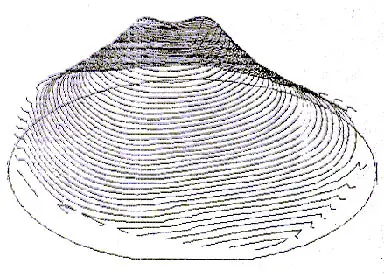
Fracture markings on a broken edge. The curved rib lines show that the leading edge of the crack that split the silicon apart traveled from the back surface of the wafer upward. The more or less vertical lines are called tear marks. Tear markes are produced when the leading edge of the crack travels on more than one plane at the same time. Tear marks are generally parallel to the direction of crack travel and they radiate away from the origin of the crack.
The fracture surface is rough along the back surface of the wafer near the origin "O." An examinatin of the back surface of the wafer at "O" showed that the back side of the wafer had been scratched during fab processing. Later, a bending stress put the back surface of the wafer into tension and this caused some of the scratch cracks to propagate, breaking the wafer apart.
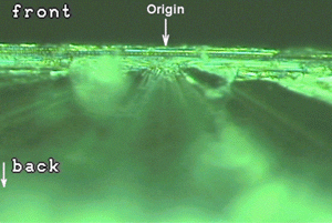
Fracture markings on a broken edge. The tear marks and other fracture markings showed that the breakage originated at the front surface of the wafer and spread downward. No wafer-weakening defect was found at the origin. In this case, the wafer was being held against a vacuum chuck by the atmospheric pressure when a wafer lifter pin came up under the back side of the wafer. The lifter pin pushed up a small part of the wafer, bending it over the lifter pin and putting the front surface into tension. The wafer broke at the front surface where the tensile stress was greatest.
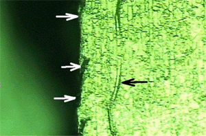
Wafer backside after backgrinding and caustic etching. Fracture analysis revealed that the origin of the breakage was at this row of caustic etched grooves. The backgrinding process created rows of extra deep cracks in the wafer backside. Caustic etching produced the grooves by etching away part of the crack damage. However, the remaining crack damage weakened the wafer and it broke apart during subsequent handling.
Descriptions and photos of fracture markings are given
in the following references:
Lawrence Dyer, Jeffrey Seaman, and Dennis Olmstead, "Hertzian Contact and Thermal Fracture of Silicon Wafers During Processing", in Semiconductor Silicon 1990, Proceedings Volume 90-7, edited by H. R. Huff, K. G. Barraclough, and Jun-ichi Chikawa, (The Electrochemical Society, Pennington, NJ, 1990), pp. 156-167.
Lawrence D. Dyer, "Fracture Tracing in Semiconductor Wafers", in Semiconductor Processing, ASTM Special Technical Publication 850, edited by D. C. Gupta, (American Society for Testing and Materials, Philadelphia, PA, 1984), pp. 297-308.
A dislocation is created when there is sufficient stress to break silicon bonds and displace silicon atoms from their normal locations. This can occur during IC fabrication due to built-in device stress, as when oxide presses against a trench sidewall or when a high concentration of small boron atoms is implanted into a volume adjacent to a volume containing larger atoms. Or dislocations can be created when furnace slip takes place due to an excessive across-the-wafer temperature nonuniformity.
The dislocation is both a structural and an electrical defect. The tube-like opening down one side of a dislocation line can act as a diffusion pipe, accelerating and channeling the diffusion of dopant atoms and producing an IC device that is shorted or that breaks down at a low voltage. The electrical properties of a dislocation can cause several types of electrical failures because a dislocation promotes recombination, conduction, and generation.
If a dislocation is present in the base of a transistor, it decreases the gain because it acts as a trap and accelerates the recombination of minority charge carriers. The dislocation line is a conductive path, and the path becomes even more conductive when metal impurity atoms become attached to the silicon atoms along the dislocation. If a dislocation ends under a gate oxide, its enhanced conductive properties can cause gate oxide integrity failure.
The most common dislocation-induced failure mechanism is leakage. For an IC device to function properly, it must be possible to effectively change the silicon into an insulator by creating a depletion region. Conduction in an MOS transistor is turned off by applying a potential to the gate to create a depletion region by pushing the majority charge carriers out of the channel. A reverse-biased P/N junction prevents current flow because the reverse bias separates the holes and electrons and creates a depletion region at the junction. However, if a dislocation threads from one electrode, through a depletion region, to another electrode, then conduction along the dislocation line causes current to flow when it should not. This is one form of dislocation-induced leakage. Leakage also occurs when a dislocation within the depletion region acts as a line of generation centers, converting thermal energy into electron-hole pairs. The electric field within the depletion region causes the electrons to flow in one direction and the holes to flow in the other direction, and this constitutes the flow of a leakage current.
Whether or not a dislocation actually causes an IC device failure depends on where the dislocation is located. If the dislocation comes up under a field oxide, for example, it does no harm. But if it threads through a P/N junction, it can cause a leakage failure. If a wafer has a high incidence of leakage failures, failure analysis can be carried out by stripping off the IC pattern layers and applying a defect etch to the silicon surface (Fig. 1). Dislocation etch pits then show where the dislocations intersected the silicon surface. If the dislocation etch pits show no across-the-wafer pattern, but are consistently located at certain IC device structures, then the stress that created the dislocations was probably built-in device stress (Fig. 2). But if the dislocations are concentrated in a center spot (Fig. 3 & 4) or an edge pattern, then the stress that created the dislocations was probably furnace stress. Often a leakage failure map will suggest whether or not furnace slip has taken place. If wafer failure analysis shows a spatial correlation between a high dislocation density and a high leakage failure rate, then you can be virtually certain that it was the dislocations that caused the leakage.
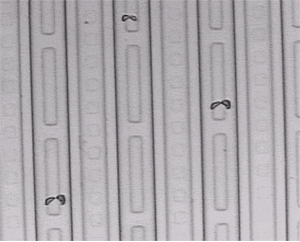
Wafer surface after pattern removal and defect etching. Short shallow dislocation loops are consistently located at certain IC device structures. This indicates that the dislocations were probably produced by built-in device stress.
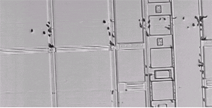
Wafer surface after pattern removal and defect etching. Dislocation etch pits are located along slip lines. This indicates that the dislocations were produced by a nonuniform temperature distribution during furnace processing.
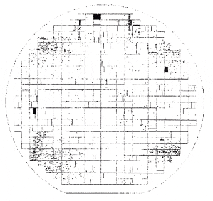
Leakage failure map. This "four corners" leakage failure pattern for a <100> wafer indicates that the wafer probably slipped at the edges due to too-rapid edge-first heating during furnace processing.
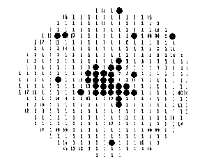
Leakage failure map. This "center spot" leakage failure pattern indicates that the wafer may have slipped in the center due to too-rapid edge-first cooling during furnace processing.
With the implementation of CMP planarization processes for Shallow Trench Isolation, the nanotopography of the silicon wafer is becoming a more significant factor to consider. Nanotopography is defined as the deviation of a surface within a spatial wavelength of around 0.2 to 20 mm. Nanotopography bridges the gap between roughness and flatness in the topology map of wafer surface irregularities in spatial frequency. Nanotopography of the silicon wafer is dictated to a large extent by the polishing process. A true planetary, freefloating, double-sided polishing process that polishes both sides of a silicon wafer simultaneously technically achieves the best nanotopography and flatness results.
Description:
With the implementation of CMP planarization processes for Shallow Trench Isolation(1), the nanotopography of the silicon wafer is becoming a significant factor to consider.
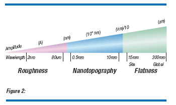
Nanotopography is defined as “the deviation of a surface within a spatial wavelength of around 0.2 to 20 mm.”(2) This is a parameter that measures the front-surface, freestate topology of an area which can range in size from fractions of a millimeter to tens of millimeters. In this sense, nanotopography differs from front-referenced site flatness in that for nanotopography the wafer is measured in a free state, while for flatness it is referenced to a flat chuck. A wafer may have perfect flatness (in the classical definition of flatness), yet still have nanotopography. If a wafer has surface irregularities on the front and backside of the wafer, but front and back surfaces are parallel, the wafer has perfect flatness. However, the same wafer will exhibit nanotopography (Figure 1). Nanotopography bridges the gap between roughness and flatness in the topology map of wafer surface irregularities in spatial frequency (Figure 2). As linewidths shrink, with non-uniform pattern density and with the use of hard pads for CMP, nanotopography may significantly degrade the dielectric film uniformity.(3,4)
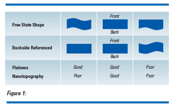
Nanotopography is measured by two techniques: light scattering and interferometry. Light scattering tools typically employed for particle and surface-defect characterization can be used to measure the local slope change over the entire surface of the wafer. The local slope change may be integrated to yield height or topography information. Since the beam size can be on the order of fractions of a micron, nanotopography can be measured. Optical interference measurement is straightforward: a beam is split into two components; one component is reflected from the wafer surface, while the second is reflected from a reference mirror; the interference of the combination of the two beams is a measure of the topology of the wafer surface. With both techniques signal filtering is used to separate the low-wavelength features (i.e. warp) so that only the high-wavelength/low-frequency information, (i.e. the true surface nanotopography) is measured.
Role of Nanotopography in CMP:
The interaction between nanotopography upon film removal uniformity in CMP has been under extensive investigation by Boning and co-workers(5,6,7,8) and Tamura et al.(9) The primary effect of oxide uniformity removal is due to the hardness of the CMP pad. The fundamental concept is very simple: soft polishing pads conform to local topology variations (i.e. nanotopography) while hard pads do not. Figure 3, adapted from Boning et al.(6), illustrates this principle. Typically, a wafer has a characteristic nanotopography length (NL, shown in the top illustration of Fig. 3). The soft pad will conform over the nanotopography and maintain a uniform film. The hard pad will not conform to the nanotopography and produce a non-uniform film with high spots on the wafer surface having a thinner film and low spots having a thicker film. Traditionally soft pads have been used for film removal CMP. However, with the need for better planarization, because of more layers, smaller CD and for multi-function logic devices which have several different areas of varying pattern densities(10), stiff pads are required. To some extent, the effect of nanotopography can be minimized by using polishing additives, such as ceria particles(11). Nonetheless wafer nanotopography becomes increasingly important.
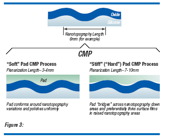
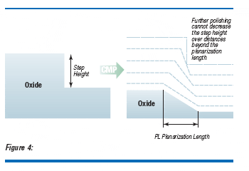
To understand the influence of nanotopography in CMP film removal uniformity, the concept of planarization length should be considered(5). The planarization length (PL) is the spatial length at which polishing cannot reduce the step height of a feature in the film thickness. This is illustrated in Figure 4. The important aspect to consider is when PL is less than NL the film uniformity is maintained. When PL is more than NL one finds nonuniform film removal. Two typical examples are shown in Fig. 3. The CMP process and the film uniformity specifications may be considered to determine the level of nanotopography required.
Impact of the Wafer:
Nanotopography of the silicon wafer is dictated to a large extent by the polishing process. For single-sided polished (SSP) wafers, the polishing process has been optimized to minimize nanotopography. In this process, to achieve good flatness, the wafer must be mounted or chucked against a flat reference block. Since the wafer backside is etched (not polished smooth), it has surface topology. Because of the fixturing process used to mount the wafers (e.g. wax mounting or vacuum chucking), the topology of the backside of the wafer and the fixturing surface and or adhesive/wax are transmitted to the front side and causes nanotopography. The other technique of mounting a wafer (the one that is normally used in CMP), viz. free mounting, does not cause nanotopography formation, but also does not guarantee the wafer is made flat. The best flatness and nanotopography is obtained when the wafers are double-sided polished (DSP). The true, planetary, free-floating DSP polishing process polishes both sides of a silicon wafer simultaneously. Since the wafer is polished in a free state, nanotopography is minimized. Also, good flatness is achieved. Thus, both good flatness and nanotopography are produced. Figure 5 shows a comparison of SSP and DSP mounting techniques and how these affect nanotopography and flatness.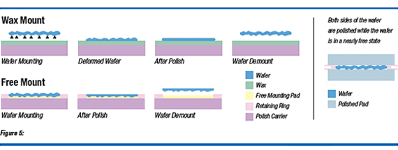
Figure 6 shows how SSP and DSP wafers affect CMP film removal uniformity. The CMP process employed (hard pad vs. soft pad) and the wafer type (SSP vs. DSP) interact with different levels of film removal uniformity. The correlation coefficients shown in this figure are taken from Boning et al.(6) They represent a measure of how much nanotopography correlates with film removal uniformity. A coefficient of 1 indicated that each high spot on the wafer surface corresponds with a local thin film (high removal or overpolish) and each low spot on the surface corresponds with a local thick film (low removal or underpolish). Conversely, a correlation coefficient of 0 indicates no correlation between nanotopography and film removal uniformity. It should be emphasized that the coefficient is not a measure of the actual uniformity, only the correlation between uniformity and nanotopography. The removal uniformity is generally better for the DSP wafer because it exhibits less nanotopography and hence less variation.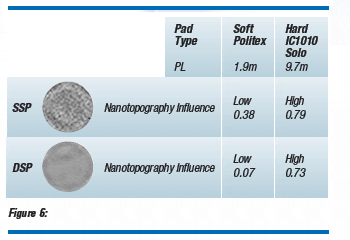
GlobalWafers has developed a planetary DSP polishing process that provides wafers with leading edge nanotopography and flatness characteristics that meet all of the increasingly demanding CMP requirements. While planetary DSP is technically the best method to achieve superior nanotopography and flatness, there are several barriers to practically implementing this method in the fab. These barriers include cost of ownership for DSP, issues related to running both a polished backside DSP and an etched backside wafer in their lines at the same time, such as electrostatic chuck problems, and in-line sensor calibration. GlobalWafers is actively exploring both planetary DSP and SSP methods that promise to achieve a good balance between nanotopography and flatness results and cost of ownership.
References:
- J. Schlueter, “Trench Warfare: CMP and Shallow Trench Isolation,” Semiconductor International, October 1999.
- SEMI DRAFT Document 3089: Guide for Reporting Wafer Nanotopography.
- K. V. Ravi “Wafer Flatness Requirements for Future Technologies,” Future Fab International, Issue 7, 207.
- C. Shan Xu, E. Zhao R. Jairath and W. Krusell, Electrochemical and Solid-State Letters, 1 (4) 181 (1998).
- B. Lee, D. Boning, W. Baylies, N. Poduje, P. Hester, Y. Xia, J. Valley, C. Koliopoulus, D. Hetherington, H. Sun, M. Lacy, “Wafer Nanotopography Effects on CMP: Experimental Validation of Modeling Methods,” Materials Research Society (MRS) Spring Meeting, San Francisco, CA, April 2001.
- D. Boning, B. Lee, W. Baylies, N. Poduje, P. Hester, J. Valley, C. Koliopoulos and D. Hetherington, “Characterization and Modeling of Nanotopography Effects on CMP,” International CMP Symposium 2000, Tokyo, Japan, Dec. 4, 2000.
- C. Oji, B. Lee, D. Ouma, T. Smith, J. Yoon, J. Chung, and D. Boning, “Wafer Scale Variation of Planarization Length in Chemical Mechanical Polishing,” J. Electrochem. Soc. 147 (11) 4307, Nov. 2000.
- B. Lee, T. Gan, D. Boning, P. Hester, N. Poduje, and W. Baylies, “Nanotopography Effects on Chemical Mechanical Polishing for Shallow Trench Isolation,” Advanced Semiconductor Manufacturing Conference, Boston, MA, Sept. 2000.
- N. Tamura, H. Niwa, M. Hatanaka, M. Kase, and T. Fukuda (Fujitsu Limited), “The Influence of Wafer Nanotopology on Residual Film Thickness Variation after Chemical Mechanical Planarization,” 197th ECS Meeting, Toronto, Ontario, Canada, May 2000.
- T. Tugbawa, T. Park, B. Lee, D. Boning, P. Lefevre, and L. Camilletti, “Modeling of Pattern Dependencies for Multi-Level Copper Chemical-Mechanical Polishing Processes,” Materials Research Society (MRS) Spring Meeting, San Francisco, CA, April 2001.
- B. Lee, D. Boning, L. Economikos, “A Fixed Abrasive CMP Model,” Chemical Mechanical Polish for ULSI Multilevel Interconnection Conference (CMP-MIC 2001), pp. 395- 402, Santa Clara, March 2001.
The Control of Oxygen Precipitation and the Impact of Internal Gettering
Vacancy concentration profiles result in ideal precipitation for gettering.
- Controlling oxygen behavior in silicon wafers via vacancy profiles is more cost-effective than conventional out-diffusion and renucleation methods.
- Proper vacancy programming forces the wafer to behave in a specific wa
- The vacancy-based approach greatly simplifies the use of silicon by decoupling the formation of the IG structure from the details of the thermal process used in device fabrication.
Controlling oxygen behavior in silicon is undeniably one of the most important challenges in semiconductor materials engineering. In particular, control of oxygen precipitation is essential for the development of internal gettering (IG) in IC manufacturing. Gettering schemes play an important role in yield management in IC manufacturing. In the 20 or so years since the discovery of the IG effect silicon wafers, many scientists and engineers have struggled with the problem of precisely and reliably controlling the precipitation of oxygen that occurs in silicon during the processing of wafers into integrated circuits. This has met with only partial success, in the sense that the “defect engineering” of conventional silicon wafers is still an empirical exercise. It consists largely of careful, empirical tailoring of wafer type (oxygen concentration, crystal-growth method, and details of any additional preheat treatments, for example) to match the specific process details of the application to which the wafers are submitted, in order to achieve good and reliable IG performance.
Reliable and efficient IG requires the robust formation oxygen-precipitate-free surface regions (“denuded zones”) and a bulk defective layer consisting of a minimum density(1) (at least about 108cm-3) of oxygen precipitates during the processing of the silicon wafer. Uncontrolled precipitation of oxygen in the near-surface region of the wafer represents a risk to device yield. The basis of the conventional method for dealing with the creation of this layered structure has been to ensure sufficient outdiffusion of oxygen from the near-surface region in order to suppress nucleation and growth. In recent years, due to radical reductions in the total thermal budgets of processes that make submicron devices, this method is no longer cost-effective.
It is possible to install vacancy-concentration profiles into silicon wafers that result in the ideal precipitation performance for IG purposes. Such an ideal vacancy profile means a high vacancy concentration in the wafer bulk and proper vacancy depletion in the near-surface region. The installation of controlled concentration profiles of vacancies is now a wafer-manufacturing process, as depicted in Figure 1. While a high concentration of vacancies enhances oxygen clustering, there is a lower bound on vacancy concentration below which clustering is “normal”. This is quite a sharp transition and lies around 5X1011cm-3. Thus a profiled vacancy concentration allows for the programming of “layered” structures — exactly what is required for the effective engineering of structures by IG. This is the basis underlying the “Magic Denuded Zone” (or MDZ) wafer.(2) A schematic illustration of this new materials-processing technique is shown in Figure 2. The use of such a vacancy-based approach greatly simplifies the use of silicon by decoupling the formation of the IG structure from the details of the crystalgrowth process, the oxygen content of the wafer, and the details of the thermal process used to fabricate the device in question.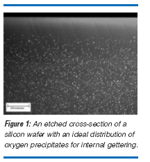
The Installation of Vacancy-Concentration Profiles in Silicon Wafers
The installation of appropriate vacancyconcentration profiles in silicon wafers is a nthree-step process, but all steps occur in a single rapid thermal processing (RTP) run.(2)
- When silicon is raised to high temperatures, vacancies and interstitials are spontaneously produced in equal amounts through Frenkel pair generation, a very fast reaction. At distances far removed from crystal surfaces, we thus have CI = Cv = {CIeq (T)Cveq(T)}1/2, where T is the process temperature. If the sample were to be cooled at this point, the vacancies and interstitials would mutually annihilate each other in the reverse process of their generation.
- In wafers, however, the surfaces are not far away, and this situation changes very rapidly. Equilibrium boundary conditions (not oxidizing or nitriding) lead to coupled fluxes of interstitials to the surface and vacancies from the surface because CIeq(T) < Cveq(T), and because of the rapid establishment of equilibrium conditions throughout the thickness of the wafer. Experiments suggest that this occurs in a matter of seconds or less. This equilibration is primarily controlled by the diffusivity of the fastest component, the self-interstitials, since the concentrations are roughly equal.
- Upon cooling, two processes are important: direct recombination of vacancies and interstitials, and diffusion of interstitials toward the surfaces. In the wafer bulk, the slower vacancies are now the dominant species of the coupled diffusion, and hence the equilibration process at the surface is not as fast as the interstitial-dominated initial equilibration. It is thus possible to “freeze-in” excess bulk vacancies at not-unreasonable cooling rates (ca. 50- 100°C/s). The residual bulk concentration of vacancies following recombination with interstitials, Cv, is the initial difference of Cveq - CIeq (at the process temperature T). Closer to the surfaces, Cv is lower, due to out-diffusion (again, primarily controlled by the dominant vacancies) toward the decreasing equilibrium values at the wafer surface. The level of bulk precipitation is controlled by the process temperature, through Cveq - CIeq, while the depth of the denuded zone is controlled by the cooling rate, through the diffusion of vacancies during cooling.
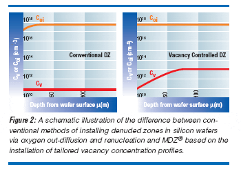
By installing a given precipitate profile into a silicon wafer, we have effectively programmed it to behave in a certain way. The precipitate profiles that result from the vacancy-programming such as is illustrated in Figure 2 produce perfect internal gettering performance reliably and reproducibly.
The denuded, or oxygen precipitate free, zone in MDZ® is a real one in the sense that the near surface density of oxygen precipitates is effectively zero. In other approaches to the problem this is not necessarily the case. For example, when oxygen precipitation enhancement is attempted at the crystal growth level, as in the case of nitrogendoped silicon, no "real" denuded zones are possible. The high temperature oxygen out-diffusion treatments which are applied to such wafers result in an "apparent" denuded zone only. The grown-in precipitates are not themselves dissolved. The oxygen concentration reduction near the surface merely restricts the size of precipitates there; at some point they cannot be detected by simple etching. But the density of oxygen related defects, in fact, remains the same -- all the way to the wafer surface. Crystal-growth based precipitation enhancement schemes increase the constraints placed on the crystal growth process. MDZ® frees the crystal growth process to be whatever it needs to be to decrease costs.
The precipitate structure is dictated by the vacancy concentration profile installed in the wafer. Proper vacancy programming forces the wafer to behave in an ideal way. It does not matter what the oxygen content of the wafer is. It does not matter what the crystal growth process was that produced the wafer -- the MDZ® process erases the crystal-history of the wafer. From an IC manufacturer's point of view, a single, highly simplified specification can now cover a multitude of applications and product ranges, hugely simplifying their use and increasing flexibility.
References:
- R. Falster, G.R. Fisher, and G. Ferrero, Appl. Phys. Lett. 59 (1991) p. 809.
- R. Falster, D. Gambaro, M. Olmo, M. Cornara, and H. Korb, in Defect and Impurity Engineered Semiconductors and Devices II, edited by S. Ashok, J. Chevallier, K. Sumino, B.L. Sopori, and W. Götz (Mater. Res. Soc. Symp. Proc. 510, Warrendale, PA, 1998) p. 27.
- R. Falster and V.V. Voronkov, “The Engineering of Intrinsic Point Defects in Silicon Wafers and Crystals”, Mater. Sci. Eng., B 73 (2000) p. 69.
Magic Denuded Zone®, MDZ®, and the MDZ logo are registered trademarks of GlobalWafers. All rights reserved. The MDZ process is protected by US patent 5,994,761 and other patents worldwide.
<100> Notch Orientation for Increased PMOS Drive Current
Benefits and Features:
- PMOS Ion increases by 10-20%
- No degradation in NMOS
- No fab integration issues or process changes are needed... wafer is still (100) surface orientation
- Applicable to multiple platforms including standard bulk wafers, SOI, and strained wafers
CMOS transistor scaling progress has been enabled by continuous reductions in channel length and gate dielectric thickness. In the sub-100nm MOSFET transistor scaling regime, fundamental limits in channel length and gate dielectric scaling are being encountered. The primary barriers to continuing scaling of planar CMOS transistors are short channel effects (SCE), which are increasingly limiting the transistor drive current improvement, and leakage current through the very thin gate dielectric. In order to manage SCE, the channel doping continues to increase. But, increasing the channel doping degrades mobility by introducing more charged impurity scattering sites. Also, the future implementation of high-K gate dielectric for control of gate leakage is known to degrade channel mobility. Because MOSFET drive current also depends on the mobility of charge carriers in the channel of the device, enabling a mobility enhancement in the device channel can offer a means to offset the negative aspects of managing SCE and gate leakage. Mobility, which describes the ease in which charge carriers drift in a semiconductor, is inversely proportional to carrier mass. Enhancing mobility (µ) enables higher MOSFET drive current which leads to higher device speed as described by the functional relationships shown below.
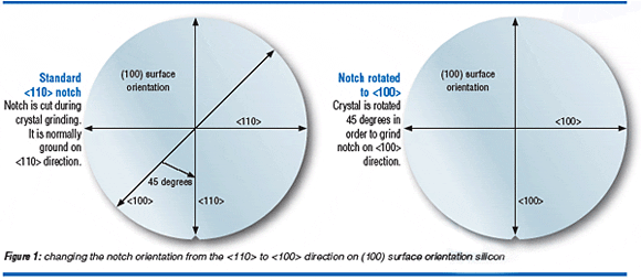
Mobility enhancement methods are the subject of an intense investigation at the starting wafer level and in the device fabrication process. The main approaches for enhancing mobility at the starting wafer level are by changing the orientation of the wafer notch, changing the wafer surface orientation, and straining the device channel. Table 1 highlights the mobility enhancement options available at the starting wafer level. The change in notch orientation from <110> to <100> is a drop-in solution that enables a 10-20% enhancement in PMOS operating current.

Several studies published in scientific literature demonstrate that orienting the PMOS channel along the <100> direction on (100) surface orientation wafers results in a gain of 10-20% in the transistor drive or “on current”(1-3). No degradation has been observed on NMOS transistors. The re-orientation of the channel directions is more easily realized by changing the starting wafer than by modifying the transistor layout methodology. The mechanism for the gain in PMOS drive current is increased mobility due to the reduction in the effective mass of holes moving along the <100> direction.
Orienting the channel direction along <100> is a simple process change in the starting wafer fabrication. Historically, the wafer flat or notch on (100) surface orientation wafer has been formed along the <110> direction at crystal grinding because these directions define the easily cleaved crystal directions of a (100) surface orientation wafer. However, since wafer dicing is done by sawing through the scribe lines orienting along <110> is no longer a technological requirement. Figure 1 shows the simple process change for rotating the crystal piece by 45 degrees at crystal grinding in order to form the wafer notch or flat along the <100> direction.
The orientation of the CMOS channel along the <100> direction offers a simple, low cost, low risk production proven enhancement of the PMOS transistor with no degradation to the NMOS transistor or complications in device process integration. It can be applied to all starting material platforms including advanced polished wafers, epitaxial wafers, and SOI wafers. The <100> notch option is already a high volume wafer fabrication process. It is a production proven starting wafer option for enhancing the performance of sub-100nm CMOS technologies. Beyond the CMOS applicability described in this note, the reorientation of the notch position to <100> has also been reported to enable improvement in the DRAM deep trench capacitor shape profiles etched into the silicon substrate, increasing cell capacitance by ~ 25%(4).
References:
- R. Khamankar et al., 2004 Symposium on VLSI Technology Digest of Technical Papers, pg 162.
- T. Matsumoto et al., 2002 IEDM Digest of Technical Papers, pg 663.
- T. Komoda et al., 2004 IEDM Digest of Technical Papers, pg 217.
- J. Amon et al., 2004 IEDM Digest of Technical Papers, pg 73.
Measurement of Interstitial Oxygen in Silicon Ingots
Increased customer confidence in process control and product capability
Benefits and Features:
- Measurement technique increases customer confidence in overall process control and product capability.
- Increases efficiency and accuracy of oxygen measurements in silicon ingots.
- Allows rapid feedback to crystal engineers in the crystal pulling area.
- Whole rod FTIR performance was demonstrated through direct correlation to conventional FTIR measurements.
Description:
Interstitial oxygen content of a silicon wafer is an important material characteristic for most modern device technologies. Interstitial oxygen in silicon is typically measured by infrared absorption using either 2 mm thick slugs or thinner product wafers. The accuracy of these measurements is subject to error. These wafer measurements are time consuming and potentially introduce handling damage or contamination to the finished polished wafer. A new infrared approach allows the measurement of interstitial oxygen in single crystal silicon. Ground, large diameter, silicon crystals are profiled for interstitial oxygen using a Fourier transform infrared (FTIR) spectrometer transmitting through full diameter crystals. Measurement intervals and sample sizes may be defined prior to the wafering process, improving assurance of product quality and allowing rapid feedback to the crystal pulling floor. Wholerod FTIR (WRFTIR) measurements can increase the producer and consumer confidence in overall process control and product capability, efficiently generating oxygen profiles along the crystal.
Technical Details:
Interstitial oxygen content of a silicon wafer is an important material characteristic for most modern device technologies.(1) Strengthening and contamination gettering properties of properly specified interstitial oxygen in silicon and their relationship to device performance are well understood and published.(2) Oxygen is incorporated in the silicon lattice during the growth process by dissolution of the quartz crucible.
Interstitial oxygen in silicon is typically measured by infrared absorption using either 2 mm thick slugs or thinner product wafers.(3,4) The accuracy of these slug or wafer measurements is subject to error unless both sample surfaces are polished, creating a more predictable optical transmission and internal reflection condition.(5) In addition, the crystal-pulling engineer may not fully understand the oxygen variation of the process unless most of the wafers are measured and the crystal oxygen profile is reassembled in a database. These wafer measurements are time consuming and potentially introduce handling damage or contamination to the finished polished wafer.
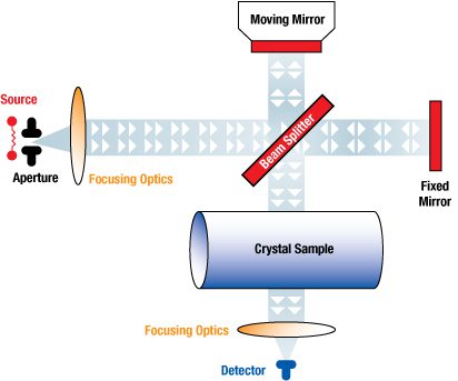
A new infrared approach allows the measurement of interstitial oxygen in single crystal silicon. Ground, large diameter, silicon crystals are profiled for interstitial oxygen using a Fourier transform infrared spectrometer transmitting through full diameter crystals.(6) Measurement intervals and sample sizes may be defined prior to the wafering process, improving assurance of product quality and allowing rapid feedback to the crystal pulling area. Whole-rod FTIR (WRFTIR) measurements will increase the producer and consumer confidence in overall process control and product capability, efficiently generating oxygen profiles along the crystal (Figure 1).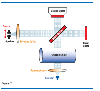
Measurement Principles:
Routine measurement of interstitial oxygen in silicon wafers utilizes infrared absorption at 1107 cm-1 (9.03 µm). This is the absorption band associated with anti-symmetric vibration of SiO2 in the silicon lattice.(7) The infrared beam passes through a wafer sample from the front to the back (Figure 2). An absorbance spectrum of an oxygen-free, float zone reference sample is “subtracted” from the sample spectrum to remove interference from multiplephonon excitations of silicon near that band. Commercially available FTIR systems simulate the subtraction process in various ways for rapid measurement of the oxygen content. Quantitative evaluation of interstitial oxygen in wafers also requires accurate understanding of the measurement effects of sample thickness, surface finish, and dopant concentration. Dopant atoms like boron or phosphorus absorb infrared light and limit the usable range of infrared analysis.(8)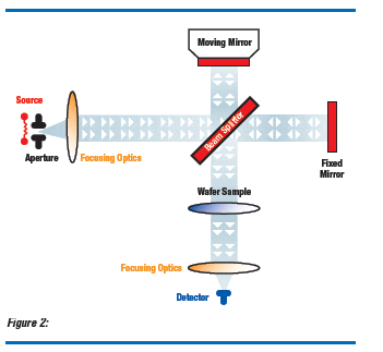
In the WRFTIR method, an infrared beam passes through a full crystal diameter, shown in Figure 1. The resulting absorbance spectrum represents the average interstitial oxygen content through one crystal diameter. This measurement uses a less intense, 1720 cm-1 (5.81 µm) absorption band that is a re-occurrence of the 1107 cm-1 band in silicon.(9,10)
Although interference from multiple-phonon excitations of silicon is negligible near the 1720 cm-1 band, the band intensity is too low to be useful in wafer measurements. When measuring through a large diameter silicon crystal, however, the cumulative absorbance is enough to provide a strong measure of interstitial oxygen content with little interference.
No measurement is possible in a full diameter crystal using 1107 cm-1 light because almost none of it passes through the whole crystal. Likewise, absorption at 1720 cm-1 is too weak to provide a measurable absorption peak when the path length is a wafer thickness (Figure 3). A long path length with low absorption provides a good combination for accurate WRFTIR measurements.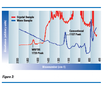
Instrumentation:
GlobalWafers has developed specifications for a WRFTIR system over the past few years. BioRad Laboratories further refined and fabricated the system and sells it as the QS-FRS. The instrument employs a standard 300 series optical bench mounted on a rail assembly. A mercury cadmium telluride (MCT) detector was selected for its excellent response and sensitivity characteristics.
The system is capable of measuring up to five crystal segments with a total length of 1.8 meters. These crystals remain fixed as the FTIR measures a specific point, processes data and moves to the next specified point. Collection conditions and spatial frequency of data along the crystal length are operator controlled. Instrument software allows definition of resolution, collection time, calibration, and spacing among adjacent measurement locations.
Experiment Design:
WRFTIR performance was demonstrated through direct correlation to conventional, wafer FTIR measurements. Sixteen p-type and four n-type, 200 mm diameter silicon crystals were selected to create a range of resistivity and oxygen values. The resistivity of the crystals ranged from 3.1 ohm-cm n-type to 56 ohm-cm p-type with the corresponding dopant density of 3.1531015 to 2.3831014 atoms per cm3. The interstitial oxygen ranged from 11 to 17 ppma (ASTM F1188). Of these twenty crystals, growth controls for four crystals were intentionally altered to create large oxygen variations along the crystal length (Figure 4). These profile variations provided a natural dispersion in the data to be discriminated by the two methods. The fulllength crystals were cut to usable lengths and ground to a nominal, 200 mm diameter.
Crystals were measured at 5 mm increments along the length and repeated twice at each defined measurement location. A single WRFTIR measurement was based on 64 scans of the FTIR mirror to calculate the absorbance spectrum. The ground crystals were subsequently processed into double side polished wafers. Wafer samples were selected at 50 mm intervals along the crystal and measured for interstitial oxygen with conventional FTIR techniques. Calibration of the WRFTIR and the conventional FTIR was performed with certified NIST traceable standards.
Three different 200 mm products were selected by resistivity specifications to support a confirming production experiment. Wafer oxygen distributions, measured on random samples using conventional FTIR techniques, were compared to “simulated distributions” derived through WRFTIR analysis.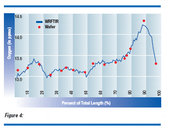
Results and Discussion:
Exact positions from the WRFTIR oxygen profile have been compared to corresponding double-side polished wafers selected from the crystals and measured by conventional methods. Excellent agreement was achieved between the WRFTIR and double-side polished wafercenter oxygen shown in Figure 5, shown on the next page. The red points correspond to high resistivity (low doping) samples, and the blue points correspond to low resistivity (high doping) samples. Clearly, free carrier absorption interferes with the oxygen measurement. Wafer radial oxygen variation, considered to be a potential source of interference, is insignificant for typical oxygen gradients produced today.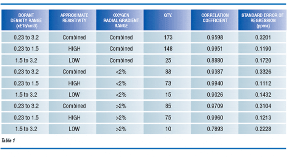
Regression statistics were calculated for various subsets of the data set to demonstrate the magnitude of carrier concentration interferences. Various regression combinations of resistivity subsets (all, high or low) and wafer oxygen radial gradient subsets (all, <2% or >2%) are provided in Table 1. Each regression analysis combining high and low resistivity subsets demonstrates significantly higher standard error. Only slight degradation in correlation occurs in cases that include oxygen gradients greater than 2%.
These correlation results suggest that accurate WRFTIR calibration is possible for predicting wafer center oxygen. At least two calibration options are required to assure accuracy over the normal working resistivity range. Additional WRFTIR calibration factors or algorithms for carrier concentration may be applied if subsequent testing suggests a need.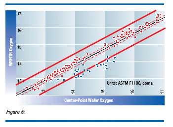
Conclusion:
Average interstitial oxygen can accurately be measured in full diameter, 200 mm silicon crystals using the 1720 cm-1infrared absorption band. The technique provides the crystal engineer rapid feedback for continuous process improvement and control. The method gives an increased understanding of the complete oxygen distribution. Accurate calibration to NIST certified standards and routine use of the WRFTIR has been demonstrated with minimal interference from radial oxygen gradient and predictable interference from resistivity over a wide range of product specifications.
Acknowledgments:
We gratefully acknowledge the contributions to this work from R. Prasad Dasari and K. Krishnan of BioRad. Portions of this article was published in the June 2000 issue of Semiconductor International. We would like to thank them for allowing us to reproduce portions of the article for this Applications Note.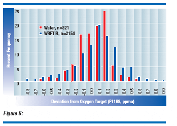
References:
- J.C. Mikkelsen, JR., Material Research Society Symposium Proceedings, Vol. 59, pp. 19-30, 1986.
- F. Shimura (ed), Oxygen in Silicon, Academic Press, 1994
- Hidenobu Abe, Isamu Suzuki, and Hiroshi Koya, “The Effect of Hydrogen Annealing on Oxygen Precipitation Behavior and Gate Oxide Integrity in Czochralski Si Wafers,” J. Electrochem. Soc., Vol. 144, No.1, pp. 306-310, 1997.
- K. Krishnan, Material Research Society Symposium Proceedings, Vol. 83-9, pp. 285-292, 1983.
- L. Koster, and F. Bittersberger, Material Research Society Symposium Proceedings, Vol. 262, pp. 271- 276, 1992.
- Joseph C. Holzer, Harold W. Korb, and Klaus Drescher, Unites States Patent #5,550,374, GlobalWafers, 1996.
- Bernard Pajot, and Bernard Cales, Material Research Society Symposium Proceedings, Vol. 59, pp. 39-44, 1986.
- F. Shimura, Semiconductor Silicon Crystal Technology, Academic Press, Inc. , pp 228-233, 1988.
- B. Pajot, H.J. Stein, B. Cales, C. Naud, “Quantitative Spectroscopy of Interstitial Oxygen in Silicon,” J. Electrochem. Soc., Vol. 132, No.12, pp. 3034-3037, 1985.
- John R. Ferraro and K. Krishnan, Practical Fourier Transform Infrared Spectroscopy, Academic Press, Inc., pp. 296-328, 1989.
- Bio-Rad Semiconductor Division, 237 Putnam Avenue, Cambridge Massachusetts 02139, U.S.A.
Silicon Manufacturing
Our silicon wafers fall into one of three general types: Prime Polished, Epitaxial, and Test/Monitor wafers. They are also differentiated by product or process type, and diameter; 150mm, 200mm, and 300mm.
Our silicon wafers vary in diameter, surface features (polished or epitaxial), composition, purity levels, crystal properties, and electrical properties. They are manufactured according to the precise specifications required by our customers. Semiconductor manufacturers require wafers of larger diameter and more stringent technical specifications in order to produce increasingly complex semiconductor devices such as the larger megabit memory chips and microprocessors.
Our customers have increased their focus on efficient semiconductor production processes because their manufacturing processes for semiconductor devices have become more expensive. Our customers make many semiconductor devices, or chips, from the same wafer, and all chips from a particular wafer are manufactured and processed simultaneously at each stage in the device manufacturing process. Because of this, larger-sized wafers allow for a greater throughput from the same semiconductor manufacturing process and allow semiconductor manufacturers to spread their fixed costs of production over a larger volume of finished products.

For example, a 6-inch (150mm) wafer has a surface area of approximately 27.4 square inches, whereas an 8-inch (200mm) wafer has a surface area of approximately 48.7 square inches. Thus, the 8-inch wafer has approximately 78% more surface area than the 6-inch wafer. A 12-inch (300mm) wafer has a surface area of approximately 109.6 square inches or approximately 125% more surface area than an 8-inch wafer. Despite the industry's focus on larger diameter wafers, we continue to manufacture and sell a significant amount of 6-inch (150mm) wafers.
The first, and most critical step in the manufacturing of silicon wafers, is the "growth" of single crystal silicon. To begin, the raw material "polysilicon" is carefully stacked by hand inside a quartz crucible, which in turn, rests inside the furnace tank of a Crystal Puller. A small amount of "dopant" (electrically active elements) such as arsenic, boron, phosphorous or antimony is added to the polysilicon. This dopant predetermines the electrical properties, or resistivity of the wafers sliced from the crystal. The machine is tightly sealed, purged to eliminate gas impurities, then fired with a "recipe" for that particular customer specification.

| As the furnace heater ramps to temperature, the crucible begins clockwise rotation. Once the melt has reached the desired temperature, a counter-clockwise, rotating silicon "seed" crystal is lowered into the molten polysilicon. The melt is slowly cooled to the recipe's temperature as crystal growth begins around the seed. The seed is then slowly raised or "pulled" from the melt - giving the appearance of controlled freezing. The temperature of the melt and the speed of extraction govern the diameter of the crystal. Once the desired diameter is achieved, the crystal-puller's advanced control systems maintain the diameter throughout the growth stage. A gradual and tapered cone finishes the crystal growing cycle in order to ensure the crystal's structural integrity. The crystal is allowed to cool before it is extracted from the crystal-puller for further processing. | 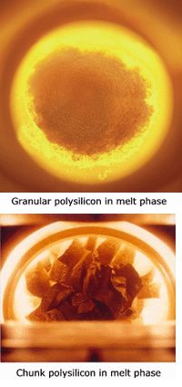 |
The crystal becomes an "ingot" only after the seed-end (the top) and the tapered-end (the bottom) are removed using an inner-diameter (ID) saw. These ends are sometimes discarded; however, to avoid a complete material loss, some ends are re-melted and used in future crystal specifications. After the ends are cut-off, the ingot is cut into shorter sections in order to optimize the slicing operation that will follow later. Next, each section is ground to the specified diameter on a mechanical lathe. A thick "slug" is taken at the end of each ingot for quality control and testing. This includes measurement of resistivity, oxygen, carbon, and bulk defects. The whole ingot is then x-rayed to confirm crystal (atomic structure) orientation.
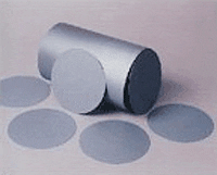
Following x-ray, the ingot is mounted on a carbon "block" using an epoxy resin. It is carefully mounted according to its orientation. The resin is allowed to cure before the ingot proceeds to slicing.
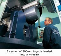
Silicon wafers are sliced from the ingot using both ID and Wire type saws. The ID saw can produce only single wafers at a time. The Wire saws are more efficient because we are able to slice the entire ingot at once. After the epoxy has cured, the ingot section is inverted and mounted into the 10-ton Wire saw. The ingot is gradually lowered into a "web" of fast moving, ultra-thin wire. The cutting action is created by pouring an abrasive slurry on the wire web, which is actually a single wire being fed from one spool to another. Immediately after slicing, the "as-cut" wafers are cleaned in a series of chemical baths to remove any residual slurry. From here, the wafers proceed into a series of refining steps to make them stronger and flatter.
First, the sharp, fragile edges are rounded or "profiled" to provide strength and stability to the wafer. This will ultimately prevent chipping or breakage in subsequent processing. Next, each wafer is laser-marked with very small alphanumeric or bar code characters. This laser-mark ID gives full trace-ability to the specific date, machine, and facility where the wafers were manufactured. The wafers are then loaded into a precision "lapping" machine that uses pressure from rotating plates and an abrasive slurry to ensure a more uniform, simultaneous removal of saw damage present on both front and backside surfaces. This step also provides stock removal and promotes flatness uniformity - a critical foundation for the polishing manufacturing process.
Now the wafers must go through an "etching" cycle. Chemical etching is necessary for the removal of residual surface damage caused by lapping; it also provides some stock removal. During the etching cycle, wafers progress down another series of chemical baths and rinse tanks with precise fluid dynamics. These chemical solutions produce a flatter, stronger wafer with a glossy finish. All wafers are then sampled for mechanical parameters and for process feedback.
Polishing the wafer gives it the mirrored, super-flat surface required for the fabrication of today's advanced semiconductor devices. It is an automated, multi-step process using ultra-fine slurry and pressure against two rotating surfaces (similar to lapping). This is accomplished using our proprietary, ninth-generation polishing machines with an innovative, chemical-mechanical polishing process pioneered by GlobalWafers in the 1960's. This form of polishing allowed solid state devices to move from individual circuits to the complexities of today's integrated circuits. Forty years later, it remains the industry standard for polishing silicon wafers.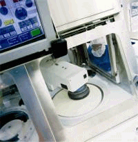
From polishing, the wafers proceed into a series of cleaning systems. The first system consists of sequential immersion tanks designed to remove residual slurry, wax and larger contaminants. This "pre-clean" step is essentially preparing the wafers to enter our world-class clean room environment.
The "final" cleaning stage is yet another series of baths. These more advanced chemical baths are optimized to remove any metallic contamination and remaining particulate. Bath temperatures, chemical mixing and filtration are all carefully controlled by a sophisticated computer system monitoring every parameter of the cleaner. The wafers emerge from final cleaning as the flattest and cleanest wafers in the world.
Before the wafers continue on to either packaging or Epitaxy, they are 100 percent inspected on the latest generation of electronic particle detection tools.
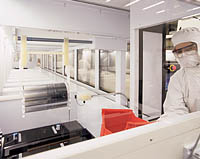
Prime polished wafers are transferred to the epitaxial furnace area inside the clean room. Epitaxy is a process that grows a thin, ultra-pure layer of silicon on the polished surface of a silicon wafer substrate. Polished wafers are loaded into single slice, or multiple slice capacity, "epi" reactor. The recipe, or customer specification, is programmed for that machine's run (cycle). Trichlorosilane gas is injected at a high-temperature as the wafer spins in the reactor. The gas flows over the top resulting in the silicon atoms adhering to the crystalline wafer structure. This "epi" layer is designed to have different compositional and electrical properties from the underlying wafer, tailored to the specific demands of the device.
The epi layer is also free of imperfections that may cause device failure and it provides increased reliability during the fabrication process. In short, epi wafers provide our customers with a technically superior wafer on which to build the most complex and sophisticated devices in the world.
GlobalWafers played an integral role in the development of Epitaxy for CMOS applications in 1982 -- a major turning point in the semiconductor industry. By applying an epitaxial layer to the surface of a silicon wafer, this pioneering work by GlobalWafers made advanced applications possible.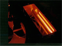
- If you DON’T measure it, you CAN’T control it.
- If you CAN’T measure it, you CAN’T control it. And...
- If you CAN’T measure it RELIABLY, you only think you're in control.
Why Measure?
- Improve Process Capability
- Reduce Process Variation
- Reduce Production Cost
- Associate Wafer Parametrics with Customer Applications
Critical Wafer Characteristics
- Edge Exclusion
- Particles and Defects
- Surface Metals
- Flatness
- Nanotopography
- Interstitial Oxygen
- Shape / Bow / Warp
- Oxidation Defects
- Lifetime
- Epi Layer Thickness
- Epi Layer Resistivity
- Dimensional Parameters
- Bulk Resistivity
- Bulk Iron
Particle and Defect Characterization – Principles of Operation
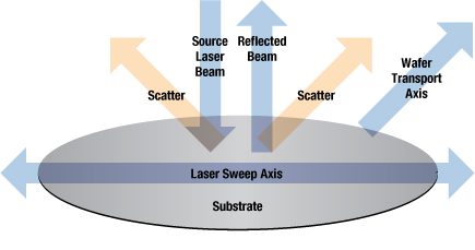
For certification requirements, wafers are 100 percent inspected using the latest particle detection tools. These tools use a scanning laser beam that sweeps the wafer's surface. Any particles present on the wafer surface will scatter the incident laser beam. By measuring the reflected light, it is possible to "map" the number, size and location of any particles.
Initial Oxygen Characterization
Interstitial oxygen content of a silicon wafer is an important material characteristic for most modern device technologies. Interstitial oxygen in silicon is typically measured by infrared absorption using either 2 mm thick slugs or thinner product wafers. The accuracy of these measurements is subject to error. These wafer measurements are time consuming and potentially introduce handling damage or contamination to the finished polished wafer. A new infrared approach allows the measurement of interstitial oxygen in single crystal silicon. Ground, large diameter, silicon crystals are profiled for interstitial oxygen using a Fourier transform infrared (FTIR) spectrometer transmitting through full diameter crystals. Measurement intervals and sample sizes may be defined prior to the wafering process, improving assurance of product quality and allowing rapid feedback to the crystal pulling floor. Wholerod FTIR (WRFTIR) measurements can increase the producer and consumer confidence in overall process control and product capability, efficiently generating oxygen profiles along the crystal.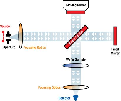
Measurement of Interstitial Oxygen in Silicon Ingots (PDF Format, 82K)
Glossary and Acronyms
PDF versions of the glossary and acronymns are furnished here, and will open in a new browser window.
Silicon/Semiconductor Glossary
GlobalWafers and Industry-related Acronyms and Symbols
6-Sigma: Capability index developed by Motorola measuring the number of standard deviations (a measure of variability) the mean is to the closest specification.
A
Å -- Angstrom
A-defects -- Dislocation loops in Silicon formed by agglomeration of interstitials
AA -- Atomic absorption
AE -- Acid Etch
AFM -- Atomic Force Microscopy
ALCVD -- Atomic Layer Chemical Vapor Deposition
AMC -- Barrel or batch type Epi reactor (Applied Materials)
APCVD -- Atmospheric-Pressure Chemical Vapor Deposition Furnace
ASIC -- Application Specific Integrated Circuit
ASM -- a single-chamber Epi reactor (ASM America)
ASTM -- American Standard Test Method
ASTM -- American Society for Testing and Materials
Acceptor: (p-type wafer) an impurity, as Gallium, Boron, etc., whose atoms in a semi-conductor produce positive, mobile charges while remaining bound in the crystal structure with a unit negative charge.
Acid: Any compound that can react with a base to form salt. Used mainly in Etching and Cleaning stages.
Alloy: Mixture of metals to increase durability.
Ambient: Natural state of the environment.
Ambient light: Normal room lighting.
Angle of Incidence: Angle in which the light goes into the wafer.
AOG: Axial Oxygen Gradient. Profile of oxygen concentration along the length of a crystal.
Argon: Inert, colorless, odorless gas used as the growing atmosphere in the crystal puller chamber; argon is backfilled after air purge.
Atmosphere: Standard barometric pressure equal to 760 torr. (1 micron = 1 millitorr, 1000 millitorr or 1000 microns = 1 torr, used as a measure of pressure).
Atomic Force Microscope (AFM): Atomic level surface mapping tool.
Autodoping: Dopant incorporated during the growth of an epitaxial layer from sources other than the dopant intentionally added to the vapor phase. Sources can include the back and front surfaces and edges of the substrate, and other substrates in the deposition assembly.
B
BESOI -- Bonded and Etch Back SOI
BGSOI -- Bonded and Grind Back SOI
BJT -- Bipolar Junction Transistor
BMD -- Bulk Micro-Defects or Bulk Microdefect Density (used almost exclusively as a measure of the oxygen precipitate density)
BOE -- Buffered Oxide Etch
BOX -- Buried Oxide Layer
BP -- Backside Polish
BV -- Breakdown Voltage
Bvox -- Breakdown Voltage-oxide
Backside: Side of the wafer that is NOT going to be polished. It is the side where the Enhanced Getter layer and/or LTO layer is placed if specified by the customer.
Backside OSF: Mechanical damage on the backside of the wafer that can precipitate stacking fault defects for gettering of impurities.
Baffle: Wafer or quartz used in furnaces to break course of gas flow at product wafers.
BDD: Bulk defect density.
BMD: Bulk Micro Defect.
Bonded Wafer: Two wafers bonded together: see SOI.
Bow: Bend or concavity of the wafer/slice. A measure of the lack of flatness of the wafer/slice.
BOX: Buried Oxide layer on SOI wafer.
Box-And-Whisker: Charting tool that visualizes data on a graph: the mean, middle 2 quartiles (50%), the upper (25%) and lower (25%) quartiles, and the largest and smallest values.
BSD: Backside damage, a process of mechanically damaging the backside of a wafer to increase gettering.
Bulk Precipitation: Defects in silicon used for gettering of impurities and can include dislocation loops, stacking fault defects, and oxygen precipitate defects.
Buried Layer: A diffused region that is covered with an epitaxial layer, subdiffused layer, or a diffusion under film.
Bvox: Breakdown voltage test of oxide layer grown on wafers, sister test to GOI.
C
oC -- Centigrade
oC/min -- Centigrade per minute
CD -- Critical Dimension
CE -- Caustic Etch
CIS -- CMOS Imaging System
cm-- Centimeter (0.01 meter)
CMOS -- Complementary Metal Oxide Semiconductor
CMP -- Chemical Mechanical Polishing
CO -- Carbon Monoxide
CO -- Carbon Dioxide
COO -- Cost of Ownership
COP's -- Crystal Originated Particles
CoQC -- Certificate Of Quality Conformance
CP -- Crystal Puller
CTL -- Charge Trap Layer
CV -- Capacity or capacitance voltage
CVD -- Chemical Vapor Deposition
CZ -- Czochralski method of pulling single crystal
Cantilever: Ceramic or silicon carbide rod or silicon carbide paddle that holds the quartz boats. This device is supported at one end. In this case, it is the door end and has the same function as a sled.
Capability Index: Value to measure how capable a product or process is at meeting a specification.
Carbon Beam: Length of carbon approximately 2" wide attached to the bottom of an ingot. In the slicing process the carbon allows the saw to cut completely through the silicon. The beam remains intact to hold the wafers until the preset number of wafers have been cut.
Carriers: Stainless steel apparatus used to contain wafers during the lapping process.
Cassette: Compact case designed to segregate slices for process handling and shipping.
Chamfer: Beveled edge.
Charge: Specified quantity of poly to be loaded into the crystal puller.
Cleanroom: Controlled areas with a low particle size/count where the latter part of wafer production takes place. The below table shows how classes are defined, with class 1 being the cleanest environment.
Class: # of particles allowed in a cubic foot of room air Particle Size
1 (means it can have no more than 1 particle) 0.5 micron or greater
10 0.5 micron or greater
100 (means it can have no more than 100 particles) 0.5 micron or greater
1000 0.5 micron or greater
10,000 0.5 micron or greater
Cleavage Plane: A break along crystal planes determined by crystal structure and always parallel to such a plane.
CMP: (Chemical-Mechical Polish) A process of removing surface material using chemical and mechanical means to achieve a mirror-like surface in preparation for subsequent processing.
Collimated Light: Light source in which the rays are parallel. Used for surface inspection of wafers.
Conductivity: A measure of the ease with which electrical carriers flow in a material: the reciprocal of Resistivity.
Conductivity Type: Defines the nature of the majority of carriers in the material: either N-type or P-type.
Contamination: Foreign matter in the silicon, other than polysilicon and dopant, that can cause loss of structure (atom alignment) during the growing process.
COP: Crystal Originated Pits.
Cp: Capability potential index which measures the width of two specifications in respect to six standard deviations.
Cpk: Statistical parameter used to compare product distribution to spec limits. A capability potential index measuring the distance from the mean to the nearest specification in respect to three standard deviations.
Crucible: Container made of quartz for holding the poly charge inside the crystal puller.
Crystal: A natural or synthetic semiconductor material whose atoms are arranged with some degree of geometric regularity. A solid composed of atoms, ions, or molecules arranged in a pattern that is periodic in three dimensions.
Crystal Puller: Machine designed to pull/grow electronic grade silicon under controlled parameters and within set specifications.
Crystallographic Orientation: There are three orientation planes in the silicon crystal: <100>, <110>, and <111>. The orientation of the wafer is classified by which orientation plane the surface of the wafer is parallel to. The surface might not be exactly parallel, but slightly different, and the difference is called the displacement angle or off angle orientation. The relationship between the crystal's orientation and the radius is marked by either a notch or a flat cut into the wafer.
Cubic Feet per Minute (CFM): Volumetric flow rate used to meter gases.
CVD (Chemical Vapor Deposition): Formation of a solid film on a substrate through the reaction of gas-phase reactants (precursors) that contain the required constituents.
Czochralski (CZ): Crystal growing process that was named after the inventor.
D
D-defects -- Very small voids in Silicon formed by agglomeration of vacancies
DIBL -- Drain Induced Barrier Lowering
DIC -- Differential Interference Contrast
DL -- Diffusion Length
DMOS -- Double-diffused MOS
DOE -- Design of Experiments
DOF -- Depth of Focus
DRAM -- Dynamic Random Access Memory
DSOD - Direct Surface Oxide Defect
DSP -- Double Sided Polish
DZ -- Denuded Zone (depth measured from the surface that is free of oxygen precipitates and which is denuded of interstitial oxygen (by out-diffusion))
Defect Free Region: The linear distance from the frontside wafer surface to the depth of the first bulk defect.
Degree: Unit of measuring angles when orienting an ingot.
Design of Experiments (DOE): Method to design, run and analyze an experiment to maximize information and minimize testing.
Diameter: Straight-line measurement drawn through the center of a circle or sphere from one side to the other.
Diffusion: A method of doping or modifying the characteristics of semiconductor material by "baking" wafers of the base semiconductor material in furnaces with controlled atmospheres of impurity materials.
Diffusion Length: The distance a front side free-electron or hole can travel through a crystal. This is proportional to the Lifetime of the crystal.
Dislocation: A class of one-dimensional, or line defects in silicon crystals.
DNZ (Denuded Zone Depth): The linear distance from the frontside wafer surface to the depth where the defect density appears nearly uniform.
Donor: Atom, usually an impurity in silicon, that acts as an electron source. It contributes an extra electron to the crystal structure. Most common is phosphorus.
Dopant: Element added to silicon decreasing its resistivity. Silicon, by itself does not conduct electricity. Boron is usually used for p-type and phosphorus is usually used for n-type.
Doping or Dopant: Chemical impurities added to polysilicon which will yield either n- or p-type silicon, depending on the specific dopant used.
E
eDRAM -- Embedded Dynamic Random Access Memory
EG -- Enhanced Gettering
EEPROM -- Electrically-erasable and Programmable Read-only Memory
EPROM -- Erasable and Programmable Read-only Memory
EOT -- Equivalent Oxide Thickness
EPI -- Epitaxy
ESF -- Epi Stacking Fault
Edge Crown: The difference between the surface elevation 1/8" (3.2mm) from the edge of the slice and the elevation of the slice edges exposed in microns (associated with epi layer deposition).
Edge Exclusion: Narrow band on the outside edge of the wafer that does not have an oxide coating.
Edge Grinding: Process that bevels the edges of the slices to strengthen them.
Ellipsometer: Optical measuring device used to measure oxide and nitride thickness, as well as, the index of refraction.
Epi: (epitaxial or epitaxy process) Depositing a thin layer of silicon atoms onto a wafer by condensing a controlled amount of silicon gas (silane) onto the polished surface of the wafer in a temperature-controlled environment.
Epitaxial Layer: The layer or layers of semiconductor material having the same crystalline orientation as the host substrate on which it is grown.
Endcone or Bottom: Gradual decreases in diameter until the silicon forms a point at the end of the growing/pulling process. As a rule of thumb, the bottom/endcone should be grown the length of the rod's diameter to allow for shock back or undesirable structure.
Etch: To remove or dissolve surface contamination, work-damaged material (polishing), and to control thickness by chemical action with strong acid and alkaline compounds.
Etch - Mirror: Used to create a clean, shiny finish for visual inspection and resistivity measurements.
Etch - Preferential: An etch that exhibits an accelerated etch rate along specific crystallographic planes.
Etch Rate: Rate of silicon removal in microns per minute.
F
FBE -- Floating Body Effect
FET -- Field Effect Transistor
FD-SOI -- Fully Depleted Silicon-on-Insulator
FPD -- Flow Pattern Defect (ref. Crystal)
FPD -- Focal Plane Deviation (ref. Mechanical flatness)
FRAM -- Ferroelectric Random Access Memory
FTIR -- Fourier Transform Infra-Red Spectroscopy
FZ -- Float Zone method of Crystal Pulling
Face: Parallel lines along the surface of the crystal, also known as growth lines or ZD, zero defect, lines.
Flat: Straight edge on the wafer's outer perimeter. It is used to identify certain characteristics. (AKA the JLS).
Flat (major): May be the only flat (straight edge) on the wafer. If there is more than one flat then it is the longest flat on the perimeter of the wafer.
Flat (minor): Shortest flat (straight edge) on the wafer.
Flatness: The maximum deviation of the wafer surface from a flat plane. Flatness measurement is usually done with the backside held to a flat surface (a vacuum chuck) and excludes linear thickness variations.
Focal Plane: That plane whose normal provides the shortest distance between the absolute maximum and absolute minimum on the wafer surface.
Focal Plane Deviation (FPD): Maximum deviation of the wafer surface above and below the focal plane.
FTIR: Fourier Transform Infrared, a means of measuring oxygen or carbon levels in the crystal.
G
GBIR -- Global flatness, back-referenced
GeOI -- Germanium-on-Insulator
GFA -- Gas Fusion Analysis
GOI -- Gate Oxide Integrity
GTIR -- Global Total Indicated Reading
GUI -- Graphical User Interface
Gettering: Gettering is a process that attracts contaminents and traps defects when the wafers are heated. Can be initiated through mechanical damage or interstial oxygen. Extrinsic gettering is caused by BSD. Intrinsic gettering is caused by interstial oxygen.
Global Flatness: Overall flatness of the wafer.
Grind: Abrade/remove material by grinding; rod diameter reduction method to specifications and for flattening.
GFA: Gas Fusion Analysis, a means of testing oxygen or carbon levels in the crystal.
GOI: Gate Oxide Integrity
H
H2 -- Hydrogen gas
H2O2 -- Hydrogen Peroxide
HCl -- Hydrogen Chloride
HF -- Hydrofluoric Acid
HMOS -- High-performance MOS
HR -- High Resistivity
HZ -- Hot Zone
Haze: Light scattering caused by microscopic surface irregularities (such as a high concentration of pits, mounds, small ridges, particles, etc.) on epitaxial wafers or polished slices.
Hillocks: Defect in the surface of the wafer resembling a hill; cannot be seen with the naked eye.
I
IC -- Integrated Circuits
IDM -- Integrated Device Manufacturer
IG -- Internal Gettering
IGBT -- Insulated Gate Bipolar Transistor
IQC -- Incoming Quality Control
ISO -- International Standards Organization
ITOX -- Internal Oxidation
Ingot: A semiconductor grown cylinder, polycrystalline or single crystal, generally of irregular diameter or in the as-grown state.
Integrated circuits: Tiny complex electronic components and their connections produced on a silicon slice.
Interstitial: Relating to crystalline compound in which small atoms or ions of a nonmetal occupy holes between the larger metal atoms and ions in the crystal lattice.
J
JFET -- Junction Field Effect Transistor
JLS (Joseph Larry Schaefer): Method of physically identifying a wafer. Major flats, minor flats and notches are ground on the silicon rod before it is cut. These markings identify the molecular orientation.
K
kg -- Kilogram
kN -- Kilo Newton
KOH -- Potassium Hydroxide
kP -- Kilo Pascal
KSIE -- Thousand Square Inch Equivalent
Kerf:The notch left by a saw cut; the width of a saw cut. Kerf Loss: The amount of material lost while slicing wafers. The kerf is the cut and swarf is the chips and fillings from the kerf.
L
LAD -- Large Area Defect
Lg -- Transistor Gate Length
LLS -- Localized Light Scatterers
LLPD's -- Large Light Point Defects
LPCVD -- Low Pressure Chemical Vapor Deposition
LPD's -- Light Point Defects
LPD-E -- Light Point Defect, class E (a KLA-Tencor SP1 defect class)
LPD-N -- Light Point Defect, class N (a KLA-Tencor SP1 defect class)
LPD-S -- Light Point Defect, class S (a KLA-Tencor SP1 defect class)
LPE -- Liquid Phase Epitaxy
LSE -- Latex Sphere Equivalent particle size
LSI -- Large-scale Integration
LSTD -- Laser Scattering Tomographic Detection
LTO -- Low Temperature Oxide
Lapping: Process to remove controlled amounts of silicon from the slice using a lapping compound. This process removes saw damage and positively impacts the slice's flatness.
Laser mark: Method of identification required by some customers. Series of letters and numbers inscribed onto the wafer by laser.
Lifetime: The average time a free-electron or hole can exist in a crystal, measured in seconds. Lifetime may vary within a crystal: bulk lifetime within the crystal and surface lifetime at, of course, the surface.
Linear Thickness Variation: Thickness variation within a slice whose front and back surfaces can be represented by two, nonparallel planes.
Local or Site Flatness: Flatness of specifically defined areas on the slice.
Lot: Group of wafers going to the same area with the same identities and are to be processed together.
Low Temperature Oxide (LTO): Sealant to keep the dopant in the wafer when it goes through the Epi process. It is applied in Furnace/Enhanced Gettering Area.
LPCVD: Low Pressure CVD, deposits a layer of polysilicon to the wafer, later removed by polishing. A backside layer can act as a gettering agent.
LPD: Light Particle Defect, sometimes known as particles.
M
MBE -- Molecular Beam Epitaxy
MCU -- Micro Controller Unit
MDZ -- Magic Denuded Zone (gettering)
MEMS -- Micro-ElectroMechanical System
MIM -- Metal-Insulator-Metal
MLD -- Modified Low Dose
mm -- 1/1000 of a meter and 0.03937 inch
mm/min -- millimeters per minute
MNOS -- Metal Nitride Oxide Semiconductor
MOCVD -- MetalOrganic Chemical Vapor Deposition
MODFET -- Modulation-Doped Field Effect Transistor
MOS -- Metal Oxide Semiconductor
MOSFET -- Metal Oxide Semiconductor Field Effect Transistor
MPU -- Micro Processing Unit
MRAM -- Magnetoresistive Random Access Memory
MSI -- Medium-scale Integration
MSIE -- Million Square Inch Equivalent
Melt: The pure, molten silicon from which single crystal silicon is grown in a crystal pulling furnace during the Czochralski process.
Meltdown: Changing a polysilicon charge from a solid to a liquid state by heating it in the crystal puller.
Micron: A unit of length, 1/1,000,000 (one millionth) of a meter.
MOScap: Test structure used for Bvox, GOI, VTW, and Zerbst tests. Capacitor structure: silicon wafer/gate oxide/polysilicon gate.
N
N -- Silicon doped to create excess negative charge carriers (electrons)
N+ -- Heavily doped, N-type silicon
NT -- Nanotopography
N2 -- Nitrogen gas
nm -- nanometers
NMOS -- Nc-hannel Metal Oxide Semiconductor
NPT -- Non-Punch Through
Nanotopology: Surface variations over a small area
N-Type: Property of the silicon semiconductor material. Doping with donor atoms increases the density of negative charge carriers (electrons) in the conduction band and produces an N-type semiconductor.
Neck: Portion of the crystal below the seed and above the taper. The first growth step in a crystal.
O
O2 -- Oxygen
Oi -- Interstitial Oxygen
OISF -- Oxidation-Induced Stacking Fault
OPP -- Optical Precipitate Profiler
OUM -- Ovonics Unified Memory
Ohm: Unit of electrical resistance.
Oi: Interstitial Oxygen.
Opposite End (OE): End of the grown crystal rod. Known more formally as the 'tang' portion of the rod.
Optical Comparator: Instrument held close to the wafer's edge for evaluation of the edge grinding process.
Optical Precipitation Profiler (OPP): Non-destructive measurement of bulk defects.
Orientation: Customer specified atom alignment in their crystal. Two main atom alignment plane patterns that are grown: 1-0-0 and 1-1-1.
OSF: Oxidation Stacking Faults.
Oxidation: Act of forming oxides. In silicon, oxygen impurities form oxides.
P
P -- Silicon doped to create excess positive charge carriers (holes)
P- -- Lightly doped P-type silicon wafer
P+ -- Heavily doped P-type silicon wafer
P/P+ -- Lightly doped P-type epi layer on a heavily doped P-type substrate
P/P- -- Lightly doped P-type epi layer on a lightly doped P-type substrate
P-band -- Anomalous oxygen precipitation region in vicinity of the vacancy/interstitial boundary
PD-SOI -- Partially Depleted Silicon-on-Insulator
PECVD -- Plasma Enhanced Chemical Vapor Deposition Furnace
PFRAM -- Polymeric Ferroelectric Random Access Memory
PFZ -- Precipitate Free Zone (depth measured from the surface that is free of oxygen precipitates but not necessarily depleted in interstitial oxygen)
PMOS -- P-channel Metal Oxide Semiconductor
PPB -- Parts Per Billion
PPC -- Post Polish Clean
PPE -- Personal Protective Equipment
PPM -- Parts Per Million
PPMA -- Parts Per Million Atomic
PPMD -- Parts Per Million Defective
PPT -- Parts Per Trillion
PROM -- Programmable Read-only Memory
PT -- Punch Through
P/V -- Peak to Valley measurement
PZT -- Lead Zirconate Titanate
P- : Typically P-type material with a resistance greater than 1 ohm.cm.
P+ : Typically P-type material with a resistance less than 1 ohm.cm.
P++ : P-type material highly doped with boron with a resistivity between 0.005 ohm.cm and 0.010 ohm.cm.
P-Type: Material that has free-holes created by the proper dopant.
Parts Per Million Defective (PPMD): On average, of one million parts produced, the number that are defective.
Polished Surface: The surface of a semiconductor slice that has received extensive chemical/mechanical operations to result in a mirror-like finish. This surface will then become the basis for subsequent device fabrication.
Poly Coating: During deposition stage of the Enhanced Gettering process, a fine grain polycrystalline silicon coating is deposited on the back side of wafer. It enhances the substrate properties the customer requires.
Polycrystalline silicon (poly): The raw material used in the Czochralski process in crystal pulling. The silicon lattice structure is randomly oriented in poly.
PP Box: Poly Propylene Box, the box used to store and ship polished wafers.
Precipitates: Football shaped etch artifacts when decorative etched with Wright Etch.
Q
R
RAM -- Random Access Memory
RF -- Radio Frequency
RFCMOS -- Radio-Frequency Complementary Metal Oxide Semiconductor
ROM -- Read-only Memory
RSD -- Raised Source/Drain
RTA -- Rapid Thermal Anneal
RTP -- Rapid Thermal Process
Resistivity: How much the silicon resists conducting electricity. The more it resists, the higher the resistivity. The less it resists, the lower the resistivity. Customers specify the resistivity level they want.
Rod: Ground crystal from Grinding. The rod is the raw material for Slicing.
ROG: Radial Oxygen Gradient, change in the concentration of oxygen from the center of a crystal to the edge.
RRG: Radial Resistivity Gradient, the difference between the resistivity at the center of a semiconductor slice and the value at a point, or at several symmetrically located points, away from the center of the slice, typically at half the slice radius or near the slice edge. This difference is expressed as a percentage of the center value.
S
SAC -- Submicron Application Crystal
SBIR -- Site flatness, back-referenced
SBSD -- Soft Backside Damage
SC1 -- 1st cleaning bath in the standard "RCA clean" sequence, consisting of NH4OH / H202/ H20 solution designed to remove particles from Si surface
SC2 -- 2nd cleaning bath in the standard "RCA clean" sequence, consisting of HCl / H202/ H20 solution designed to remove metals from Si surface
SCE -- Short Channel Effects
SEM -- Scanning Electron Microscope
SFQR -- Site flatness, best-fit, front-referenced
SFSR -- Site flatness, best-fit, front-referenced, scanning site
SGOI - Strained Si on SiGe on Insulator
Si -- Silicon
SIE -- Square Inch Equivalent
SIMOX -- Separation by Implantation of Oxygen
SIMS -- Secondary Ion Mass Spectroscopy
SiO -- Silicon Monoxide
SiO2 -- Silicon Dioxide
SIP -- Single In-line Package
SIRM -- Scanning Infra-red Microscope
SoC -- System-on-a-Chip
SOI -- Silicon-on-Insulator
SOS -- Silicon-on-Sapphire
SPT -- Soft Punch Through
SPV -- Surface Photovoltage
SRAM -- Static Random Access Memory
SRP -- Spreading Resistance Probe or Spreading Resistance Profile
SSI -- Small-scale Integration
sSi -- Strained Silicon
SSIS -- Surface Scanning Inspection System
SSOI -- Strained Silicon directly on Insulator
SSP -- Single Side Polish
STD -- Standard
STD CZ -- Standard Czochralski-grown Crystal
STI -- Shallow Trench Isolation
STIR -- Site TIR (Total Indicated Reading)
Secondary Ion Mass Spectrometry (SIMS): Dopant and impurity depth profiling, done by outside vendors for SunEdison Semiconductor.
Seed End (SE): Beginning end of a grown silicon crystal rod.
Seed Crystal: The seed is the starting point for growing the ingot. It must have the same crystal orientation as desired for the resulting ingot.
SEMI: Semiconductor Equipment and Materials Institute. Sets specifications for the semiconductor industry.
Silicon: Tetravalent nonmetallic element that occurs combined as the most abundant element next to oxygen in the earth's crust and is used in alloys and electronic devices.
Single Crystal: When the atoms in the crystal are all aligned in the same way.
Slip: A process of plastic deformation in which one part of the crystal undergoes a shear displacement relative to another in a fashion that preserves the crystallinity of the material. The direction is on a specific crystallographic plane.
Slug: Thick piece of silicon, usually a wedge cut, used to test the material characteristics for customer specs.
Slurry: Solid suspension in liquid used for slicing, lapping, and polishing.
SOI: Silicon on Insulator, usually achieved by bonding two wafers, one of which has oxide on top.
SRP - Spreading Resistance Profiling: The resistance measured between the conductive metal of a point probe and a large area, relatively low-resistance semiconductor contact, dominated by the resistivity of the semiconductor volume close to the problem.
Stacking Faults: Pyramid shaped imperfections in the silicon wafer.
Substrate: Basic surface on which a material adheres. A single-crystal slice that is the basis for subsequent processing operations, such as epi layer deposition, diffusion, ion implants, etc.
Surface Photovoltage (SPV): Test for recombination minority carrier lifetime.
Swirl: Shallow pits looked for during visual inspection. Helical or concentric features that are visible to the unaided eye after preferential etch, and appear to be discontinuous under 150x magnification.
T
T -- Temperature
TCS -- Trichlorosilane
TEM -- Transmission Electron Microscope
TIR -- Total Indicated Reading
TOX -- Gate Oxide Thickness
Tsoi -- Thickness of SOI top Si layer
TSOP -- Thin Small Outline Package
TTV -- Total Thickness Variation
Taper: A measure of the flatness of a wafer, taper being thicker at the edges than at the center.
Thickness: Cross sectional depth of a silicon slice measured in mils (1 mil = 0.001 inch).
TIR: Total Indicator Reading, the distance between the highest and lowest point on the wafer surface measured normal to the focal plane.
Total Thickness Variation (TTV): variation of thickness from the center and both sides of the wafer.
U
ULSI-- Ultra Large-scale Integration
V
v/G -- v: growth rate (crystal pulling rate), G: vertical temperature gradient at melt/solid interface
VI -- Vacancy Interstitial
VLSI -- Very Large-scale Integration
VPE-- Vapor Phase Epitaxy
W
WRFTIR -- Whole Rod Fourier Transform Infra-Red Spectroscopy
Warp: Maximum distance from the lowest point to the highest point on the wafer's surface.
X
XTL -- Crystal

